Hybrid RF Circuit Board 5-Layer High Frequency PCB Built on 10mil RO4350B and FR-4
(Printed circuit boards are custom-made products; the images and parameters shown are for reference only)
Introduction
Hello Everyone,
Warm greetings!
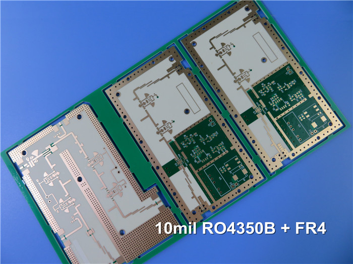
Today, we are excited to introduce a 5-layer PCB constructed from a combination of high-frequency RF material, RO4350B, and epoxy glass FR-4. This board is specifically designed for 2.4 GHz antenna applications. It has a thickness of 1.0 mm and features through holes. Both sides are covered with a green solder mask, and the pads are finished with immersion gold. These boards are fabricated according to IPC 6012 Class 2 standards using the provided Gerber data. Each batch consists of 25 boards, which are packed for shipment.
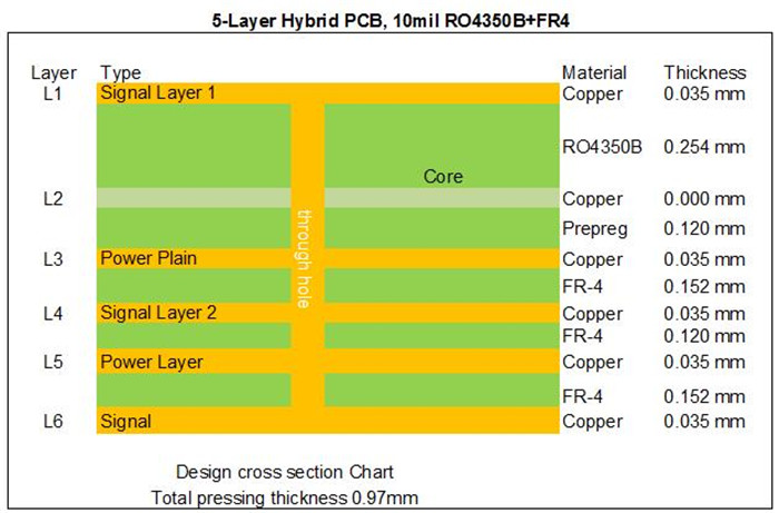
The above diagram illustrates the stack-up. “Layer 2” is etched away, leaving five layers of copper on the board.
Features and Benefits
1)Enhanced Signal Integrity: Improved performance compared to stack-ups made entirely from FR-4.
2)High Production Capacity: Our facility boasts a capability of 30,000 square meters per month.
3)Diverse PCB Types: We can produce 8,000 different types of PCBs each month.
4)Efficient Design Review: Quick CAD/CAM checking and free PCB quotations are available.
5)Flexible Order Quantities: No minimum order quantity (MOQ), making it cost-effective for prototypes and small runs.
6)Quality Standards: Adheres to IPC Class 2 and IPC Class 3 standards.
Applications
This versatile PCB is suitable for a wide range of applications, including:
consumer electronics;
Wi-Fi antennas;
8 port switches;
embedded computer DC transformers;
inverter systems;
Wi-Fi 4G routers;
temperature modules.
Parameter and Data Sheet
PCB SIZE |
159.12 x 39.78mm=1PCS |
BOARD TYPE |
Hybrid Multilayer PCB |
Number of Layers |
5 layers |
Surface Mount Components |
YES |
Through Hole Components |
YES |
LAYER STACKUP |
copper ------- 18um(0.5oz)+plate TOP layer |
RO4350B 10 mil (0.254mm) |
|
Prepreg 0.12mm |
|
copper ------- 35um(1oz) MidLayer 1 |
|
FR-4 0.152mm |
|
copper ------- 35um(1oz) MidLayer 2 |
|
Prepreg 0.12mm |
|
copper ------- 35um(1oz) MidLayer 3 |
|
FR-4 0.152mm |
|
copper ------- 18um(0.5oz)+plate BOT layer |
|
TECHNOLOGY |
|
Minimum Trace and Space: |
5 mil / 5 mil |
Minimum / Maximum Holes: |
0.4 mm / 5.0 mm |
Number of Different Holes: |
7 |
Number of Drill Holes: |
81 |
Number of Milled Slots: |
2 |
Number of Internal Cutouts: |
0 |
Impedance Control: |
no |
Number of Gold finger: |
0 |
BOARD MATERIAL |
|
Glass Epoxy: |
FR-4 Tg130℃, er<5.4; RO4350B Tg280℃, er < 3.8 |
Final foil external: |
1 oz |
Final foil internal: |
1 oz |
Final height of PCB: |
1.0 mm ±0.1 |
PLATING AND COATING |
|
Surface Finish |
Immersion gold (14.6% ) 0.05µm over 3µm nickel |
Solder Mask Apply To: |
TOP and Bottom, 12micron Minimum |
Solder Mask Color: |
Green, PSR-2000GT600D, Taiyo Supplied. |
Solder Mask Type: |
LPSM |
CONTOUR/CUTTING |
CNC Routing |
MARKING |
|
Side of Component Legend |
TOP and Bottom. |
Colour of Component Legend |
White, IJR-4000 MW300, Taiyo brand |
Manufacturer Name or Logo: |
Marked on the board in a conductor and leged FREE AREA |
VIA |
Plated through hole(PTH), minimum size 0.4mm. |
FLAMIBILITY RATING |
UL 94-V0 Approval MIN. |
DIMENSION TOLERANCE |
|
Outline dimension: |
0.0059" |
Board plating: |
0.0029" |
Drill tolerance: |
0.002" |
TEST |
100% Electrical Test prior shipment |
TYPE OF ARTWORK TO BE SUPPLIED |
email file, Gerber RS-274-X, PCBDOC etc |
SERVICE AREA |
Worldwide, Globally. |
